SPONSORED LINKS
Aureal Vortex Sound Board Chipset Technical description.
This VERY preliminary and buggy. Don't rely on this document. There is ABOSULUTELY NO WARRANTY about the content of this document. Any corrections, addition however are gladly welcome.
Preamble
This a mix of several separate pieces of documents, most of them part of the Sourceforge and Savannah disassembling project efforts. The goal of this paper is to order and combine all of the available information regarding this superb and historical important audio chipset. I would like to thank anyone involved at the Sourceforge Aureal and the Savannah OpenVortex projects.
General description
The vortex architecture consists of a variety of modules that are connected by programmable routes. Various routes are made between the these modules to produce the desired results. For example, a route can be made between a DMA controller and output codec, or from a DMA controller to a sample rate converter and then to the output codec. They can be strung together in a variety of ways.
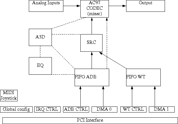

Dotted lines are possibly routeable audio data path. The existence and internals of the EQ and A3D module are very uncertain, and probably we will not be able to be used :-(
There are several i/o ports mapped to a MMIO area of different size, depending on the particular model, which are used to control and monitor the behavior of the chipset.
There are some mayor family of ports, which will be described along this document in sequence
Interrupt Control, Status and Programmable Timer Interface
AC97 Codec I/O
FIFO, ADB (Audio Data Bus) and Routing.
Sample Rate Converter
DMA controller
General Configuration Register
This is a general configuration port, which contains the following global configuration flags.
|
|
AU8810 |
AU8820 (0x1280c) |
AU8830 |
|---|---|---|---|
|
Enable glob. IRQ |
|
0x00004000 |
0x0004000 |
|
Enable MPU401 |
|
0xffffff9f |
|
|
0x330 - 0x331 |
|
0x00000600 |
|
|
0x3xx - 0x3xx |
|
0x00000400 |
|
|
0x3xx - 0x3xx |
|
0x00000200 |
|
|
(disabled?) |
|
0x00000000 |
|
|
Enable Joystick |
|
0xfffff1ff |
|
|
|
|
(PORT << 9) |
|
Interrupt Control and Status Registers
Port Numbers
Here is a table of the names (suggestions?) of the interrupt related registers for each of the Aureal chipset family.
|
Chipset |
IRQ_GLOB |
IRQ_SOURCE |
IRQ_CTRL |
IRQ_STAT |
|---|---|---|---|---|
|
AU8810 |
|
|
|
|
|
AU8820 |
0x1280c |
0x12800 |
0x12804 |
0x1199c |
|
AU8830 |
|
|
|
|
Interrupt Control
This port allows to enable or disable individual sources of interrupts, for example the MIDI port, Timer or whatever. The flags for each Interrupt source are the same as the IRQ_SOURCE flags.
Information regarding this port is not 100% tested.
|
IRQ_CTRL |
AU8810 |
AU8820 |
AU8830 |
|---|---|---|---|
|
IRQ_FATAL |
|
0x00000001 |
|
|
IRQ_PARITY |
|
0x00000002 |
|
|
IRQ_PCMOUT |
|
0x00000020 |
|
|
IRQ_TIMER |
|
0x00001000 |
|
|
IRQ_MIDI |
|
0x00002000 |
|
Interrupt Sources
There are several sources which can cause an interrupts. The IRQ_SOURCE port allows to demultiplex the different sources of interrupts; in other words, to know who produced the interrupts and needs servicing.
|
IRQ_SOURCE |
AU8810 |
AU8820 |
AU8830 |
|---|---|---|---|
|
IRQ_FATAL |
|
0x00000001 |
|
|
IRQ_PARITY |
|
0x00000002 |
|
|
IRQ_PCMOUT |
|
0x00000020 |
|
|
IRQ_TIMER |
|
0x00001000 |
|
|
IRQ_MIDI |
|
0x00002000 |
|
Interrupt Acknowledge and Timer.
The chipset has a programmable Timer, which can be programmed to generate periodic interrupts for example to update DMA buffers. The associated port has a different function for reading and writing. When read it acknowledges the current interrupt (?) and when written one can set the Timer period in 1/48000 second units. A typical value is 0x60 which equals to about 500 interrupts per second.
AC97 Codec I/O
|
Chipset |
CODEC_CTRL |
CODEC_EN |
CODEC_CHN |
CODEC_IO |
|
|---|---|---|---|---|---|
|
AU8810 |
|
|
|
|
|
|
AU8820 |
0x11984 |
0x11990 |
0x11880 |
0x11988 |
|
|
AU8830 |
0x29184 |
0x29190 |
0x29080 |
0x29188 |
|
CODEC_CTRL
A static write sequence to this port initializes the CODEC with a 5ms delay in between. This sequence are:
For AU8810: FIXME
For AU8820: 0x00a8, 0x80a8, 0x80e8, 0x80a8, 0x00a8, 0x00e8
For AU8830: 0x8068, 0x00e8
CODEC_IO
This port is used to communicate directly to the codec. To differentiate between address and command, write or read, etc, the following masks, and shift constants are used:
The write Flag, when set, indicates a write to the CODEC, if unset, indicates a read from the CODEC.
Write Flag: 0x800000
Address Shift: This is the amount by which the address has to be shifted to the left when issuing an command with an address. This implies a mask, which is given following too.
ADDRSHIFT: 16
ADDRMASK: 0x007f0000
The data is aligned to the right (data shift is zero) and is 16 bit wide:
DATSHIFT: 0
DATMASK: 0x0000ffff
CODEC_EN
This register purpose is to enable/disable the different channels of the codec. Each channel has a flag associated to it. There are only two interesting flags, for channel 0 and 1.
Channel0: 0x00000100
Channel0: 0x00000200
CODEC_CHN
The only known thing about this register is that its the base of a series of register which are initialized once and never touched again.
AU8810:
FIXME!
AU8830 and AU8820: 32 writes, following this pattern:
CODEC_CHN + 0x0 = 0x00000000
CODEC_CHN + 0x4 = 0xffffffff
CODEC_CHN + 0x8 = 0xfffffffe
CODEC_CHN + 0xc = 0xfffffffd
...
The complete initialization sequence is:
Initialize CODEC_CTRL register
Initialize CODEC_CHN registers.
Initialize CODEC_EN register.
Write again last written value to CODEC_CTRL (0x00e8 for AU8820 and AU8830).
ADB DMA Engine
The Audio Data Bus interconnects each of the Aureal chipset components. The ADB_CTRL and ADB_STATUS access the same internal register, but one is read only and the other is write only, providing complete write read access with the corresponding MMIO ports.
|
Chipset |
ADB_SMPR |
ADB_CTRL |
ADB_STATUS |
ADB_S0 |
ADB_S1 |
|---|---|---|---|---|---|
|
AU8810 |
|
|
|
|
|
|
AU8820 |
0x10a00 |
0x10580 |
0x105c0 |
0x10608 |
0x1060c |
|
AU8830 |
0x28400 |
0x27a00 |
0x27e00 |
|
|
ADB_SMPR:
The lower word of the DMA_SMPR register controls sample rate enable/disable. Each channel is assigned 2 bits. The lower bit is for enabling the mono sample rate and the upper bit for stereo sample rate.
--Example--
xxxx xxxx xxxx xxxx | 0000 0000 0000 0000 = sample rate disabled
xxxx xxxx xxxx xxxx | 0000 0000 0000 0001 = mono sample rate on first channel
xxxx xxxx xxxx xxxx | 0000 0000 0000 0010 = stereo sample rate on first channel
|
ADB_CTRL(w) |
AU8810 |
AU8820 |
AU8830 |
|---|---|---|---|
|
DMA position |
|
0x00000fff |
|
|
DMA cur. subbuffer |
|
0x00003000 |
|
|
FIFO |
|
0x0003c000 |
|
|
interrupt |
|
0x00001000 |
|
|
|
|
|
|
|
ADB_STATUS(r) |
AU8810 |
AU8820 |
AU8830 |
|---|---|---|---|
|
DMA position |
|
0xfffff000 |
|
|
DMA cur. subbuffer |
|
0x00003000 |
|
|
FIFO Control |
|
0x0003c000 |
|
|
stop |
|
0x00000000 |
|
|
start |
|
0x00020000 |
|
|
init |
|
0x00010000 |
|
|
|
|
|
|
|
|
|
|
|
|
|
|
|
|
|
|
|
|
|
WT DMA Engine
The WT DMA Engine is another audio data path presumably used for the WaveTable engine. The WT_CTRL and WT_STATUS, same as the similar ADB registers, access the same internal register, but one is read only and the other is write only, providing complete read write access with the corresponding MMIO ports. In the particular case of the AU8820, these MMIO addresses are the same.
|
Chipset |
WT_SMPR ? |
WT_STATUS |
WT_CTRL |
WT_S0 |
WT_S1 |
|---|---|---|---|---|---|
|
AU8810 |
|
|
|
|
|
|
AU8820 |
|
0x10500 |
0x10500 |
0x10600 |
0x10604 |
|
AU8830 |
|
0x27d00 |
0x27900 |
|
|
WT_SMPR:
The lower word of the DMA_SMPR register controls sample rate enable/disable. Each channel is assigned 2 bits. The lower bit is for enabling the mono sample rate and the upper bit for stereo sample rate.
--Example--
xxxx xxxx xxxx xxxx | 0000 0000 0000 0000 = sample rate disabled
xxxx xxxx xxxx xxxx | 0000 0000 0000 0001 = mono sample rate on first channel
xxxx xxxx xxxx xxxx | 0000 0000 0000 0010 = stereo sample rate on first channel
|
WT_STATUS |
AU8810 |
AU8820 |
AU8830 |
|---|---|---|---|
|
DMA position |
|
0x00000fff |
|
|
DMA cur. Sub buffer |
|
0x00600000 |
0x00003000 |
|
FIFO ? |
|
0x0003c000 |
- |
|
FIFO enabled? |
|
|
0x00200000 |
|
|
|
|
|
|
WT_CTRL |
AU8810 |
AU8820 |
AU8830 |
|---|---|---|---|
|
? |
|
0x0000f000 |
|
|
Arg 1 & 5 (int) |
|
0x00001000 |
|
|
Enforced high |
|
0x00002000 |
|
|
FIFO ? |
|
0x0003c000 |
|
|
FIFO enabled? |
|
0x00020000 |
0x00200000 |
|
|
|
|
|
|
|
|
|
|
FIFO
|
Chipset |
ADB_FIFO_CTRL |
ADB_FIFO_DATA |
WT_FIFO_CTRL |
WT_FIFO_DATA |
|
AU8810 |
|
|
|
|
|
AU8820 |
0xf800 |
0xe000 |
0xf840 |
0xe800 |
|
AU8830 |
0x16100 |
0x14000 |
0x16000 |
0x10000 |
The FIFO_CTRL registers are a set of FIFO control register, which control the behavior and status of the FIFO data. There is a set of those for the ADB and another for the WT engine.
|
FIFO_CTRL |
AU8810 |
AU8820 |
AU8830 |
|---|---|---|---|
|
set this reg. readonly |
|
0x00000001 |
0x00000001 |
|
can do CTRL |
|
0x00000002 |
0x00000002 |
|
Valid |
|
0x00000010 |
0x00000010 |
|
Empty |
|
0x00000020 |
0x00000020 |
|
? |
|
0x00010000 |
|
The FIFO data registers are the actual data registers of the FIFO. There is one FIFO for each audio data path, the ADB FIFO and the WT FIFO.
AU8830:
StartFIFO
0x27a00 = 0x22000
Enable/DisableFIFO
set the 22 bit of 0x27e00
Init
0x16100 + num*4 |= 0x41000, 42000
AU8820:
StartFIFO
0x10580 |= 0x22000
Enable Disable
Init
0xf800 + num*4 |= 0x10000
|
Chipset |
SAMPLE_TIMER |
TIMER_UNK1 |
|
AU8810 |
|
|
|
AU8820 |
0x11998 |
0x1199c |
|
AU8830 |
|
|
SAMPLE_TIMER
This register holds the sample time. This register is read only.
TIMER_UNK1
This register when read clears the Timer interrupt. When written to allows to set the timer timeout value (period). It looks like there are some flags mapped to this register, but their use is unknown.
AU8820: upper limit appears to be 0x3ffff
masks: 0x800000, 0xffffff, 0xff000000
ROUTING