SPONSORED LINKS
Aureal Vortex Sound Board Chipset Technical description.
This VERY preliminary. There is ABOSULUTELY NO WARRANTY about the content of this document. Any corrections, addition however are gladly welcome.
Author: Manuel Jander
(mjander@embedded.cl)
Preamble
This a mix of several separate pieces of documents, most of them part of the Sourceforge and Savannah disassembling project efforts. The goal of this paper is to order and combine all of the available information regarding this superb and historical important audio chipset. I would like to thank anyone involved at the Sourceforge Aureal and the Savannah OpenVortex projects.
General description
The vortex architecture consists of a variety of modules that are connected by programmable routes. Various routes are made between the these modules to produce the desired results. For example, a route can be made between a DMA controller and output codec, or from a DMA controller to a sample rate converter and then to the output codec. They can be strung together in a variety of ways.
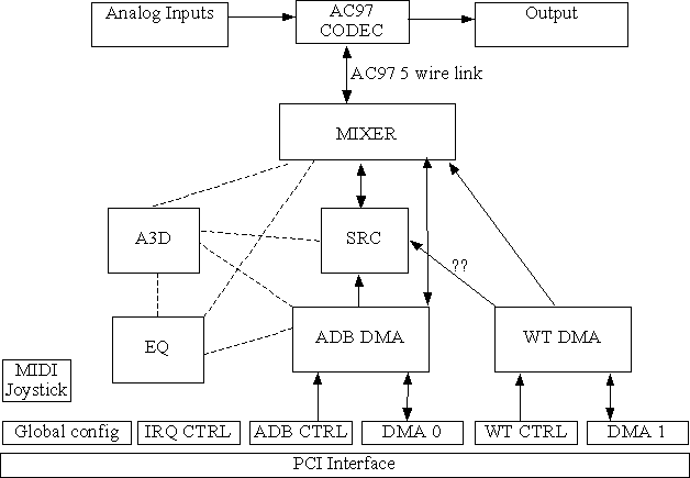
Dotted lines are supposedly possible routeable audio data path. The
existence and internals of the EQ and A3D module are very uncertain, and
probably we will not be able to be used, except if some former employee
of Aureal Semiconductors gives us a little help.
There are several i/o ports mapped to a MMIO area of different size, depending on the particular model, which are used to control and monitor the behavior of the chipset.
There are some mayor family of ports, which will be described along this document in sequence
Global configuration register
Interrupt Control, Status and Programmable Timer Interface
AC97 Codec I/O
ADB (Audio Data Bus) and WT (WaveTable)
Routing
Mixer
Sample Rate Converter
DMA controller
Global Configuration Register
This is a global configuration port, which contains the following global configuration flags.
|
bits |
AU8810 |
AU8820 (0x1280c) |
AU8830 |
|---|---|---|---|
|
Enable glob. IRQ |
|
0x00004000 |
0x0004000 |
|
Enable MPU401 |
|
0x00000001 |
|
|
MIDI Legacy port |
|
0x00000060 |
|
|
Enable Joystick |
|
0x00000008 |
|
|
Jstck. Legacy port |
|
0x00000e00 |
|
|
Addr (0x201, 0x207) |
|
(addr << 9) |
|
Interrupt Control and Status Registers
Port Numbers: Here is a table of the names (suggestions?) of the interrupt related registers for each of the Aureal chipset family.
|
Chipset |
IRQ_SOURCE |
IRQ_CTRL |
IRQ_STAT |
|---|---|---|---|
|
AU8810 |
|
|
|
|
AU8820 |
0x12800 |
0x12804 |
0x1199c |
|
AU8830 |
|
|
|
Interrupt Control
This port allows to enable or disable individual sources of interrupts, for example the MIDI port, Timer or whatever. The flags for each Interrupt source are the same as the IRQ_SOURCE flags.
|
IRQ_CTRL |
AU8810 |
AU8820 |
AU8830 |
|---|---|---|---|
|
IRQ_FATAL |
|
0x00000001 |
|
|
IRQ_PARITY |
|
0x00000002 |
|
|
IRQ_PCMOUT |
|
0x00000020 |
|
|
IRQ_TIMER |
|
0x00001000 |
|
|
IRQ_MIDI |
|
0x00002000 |
|
Interrupt Sources
There are several sources which can cause an interrupts. The IRQ_SOURCE port allows to demultiplex the different sources of interrupts; in other words, to know who produced the interrupts and needs servicing.
|
IRQ_SOURCE |
AU8810 |
AU8820 |
AU8830 |
|---|---|---|---|
|
IRQ_FATAL |
|
0x00000001 |
|
|
IRQ_PARITY |
|
0x00000002 |
|
|
IRQ_PCMOUT |
|
0x00000020 |
|
|
IRQ_TIMER |
|
0x00001000 |
|
|
IRQ_MIDI |
|
0x00002000 |
|
Interrupt Acknowledge and Timer.
The chipset has a programmable Timer, which can be programmed to generate periodic interrupts for example to update DMA buffers. The associated port has a different function for reading and writing. When read it acknowledges the current interrupt (?) and when written one can set the Timer period in 1/48000 second units. A typical value is 0x60 which equals to about 500 interrupts per second.
AC97 Codec I/O
|
Chipset |
CODEC_CTRL |
CODEC_EN |
CODEC_CHN |
CODEC_IO |
|
|---|---|---|---|---|---|
|
AU8810 |
|
|
|
|
|
|
AU8820 |
0x11984 |
0x11990 |
0x11880 |
0x11988 |
|
|
AU8830 |
0x29184 |
0x29190 |
0x29080 |
0x29188 |
|
CODEC_CTRL
A static write sequence to this port initializes the CODEC with a 5ms delay in between. This sequence are:
For AU8810: FIXME
For AU8820: 0x00a8, 0x80a8, 0x80e8, 0x80a8, 0x00a8, 0x00e8
For AU8830: 0x8068, 0x00e8
[8] -> (read) Codec ready.
?[9..21] -> slot valid tag bits.
CODEC_IO
This port is used to communicate directly to the codec, using the
output and input stream slot 1 and 2 of the AC97 codec.
Write Flag: 0x800000 = 1 << (19 + 4)
Both data and address are read and writable. After a write, the address
can be read back to ensure that the data corresponds to the command
issued before, since this is a synchronous interface.
[21..22,24..31] -> unused/unknown.
[23] -> write only: 0 = READ CMD, 1 = WRITE CMD.
[16..20] -> slot1 [12..18] addr
[0..15] -> slot 2 [4..19] data
CODEC_EN
This register purpose is to enable/disable the different channels of the codec. Each channel has a flag associated to it. There are only two interesting flags, for channel 0 and 1.
Channel0: 0x00000100
Channel0: 0x00000200
CODEC_CHN
The only known thing about this register is that its the base of a series of register which are initialized once and never touched again.
AU8810:
FIXME!
AU8830 and AU8820: 32 writes, following this pattern:
CODEC_CHN + 0x0 = 0x00000000
CODEC_CHN + 0x4 = 0xffffffff
CODEC_CHN + 0x8 = 0xfffffffe
CODEC_CHN + 0xc = 0xfffffffd
...
The complete initialization sequence is:
Initialize CODEC_CTRL register
Initialize CODEC_CHN registers.
Initialize CODEC_EN register.
Write again last written value to CODEC_CTRL (0x00e8 for AU8820 and AU8830).
ADB and WT
There are two audio engines. The ADB engine which provides 16 channels,
and the WT engine with 32 channels (48 total). Each engine uses one
single DMA buffer through which the different channels are multiplexed
(interlaced). Each DMA buffer has 4 subbuffers of a size of upto 4kB,
which can be chained in sequence or used individually.
Each block of the ADB or WT engines are routeable. The WT routing is
unknown, because it semed to have been ripped of the Linux binary
drivers.
To connect a block to another it must be done through a channel (or
bus). So the block has to enable one or more of its channel connection.
The Binary driver calls this "Enable Samplerate". The SampleRate
enable register of each block are the same, and consist of a dword
representing a bitmap for 32 channels. Some channels semes to have
special attributes, because some very specific channels are used to
connect one given block with another.
The most important blocks
of the engines are the DMA engine, SampleRateConverter, the mixer and
the Codec interface. For Playback for example the DMA engine is
connected to a SRC, the SRC output to the mixer and the mixer output to
the codec.
This is the DMA engine
that feeds the ADB engine (something). The ADB_CTRL and ADB_STATUS
access the same internal register, but one is read only and the other is
write only, providing complete write read access with the corresponding
MMIO ports.
Routing Addresses:
| Chipset |
Addresses |
|
AU8810 |
0 .. ? |
|
AU8820 |
0 .. 0x0f |
|
AU8830 |
0 .. ?
|
|
Chipset |
SR_EN |
DMA_CTRL |
DMA_STAT |
ADB_S0 |
ADB_S1 |
|---|---|---|---|---|---|
|
AU8810 |
|
|
|
|
|
|
AU8820 |
0x10a00 |
0x10580 |
0x105c0 |
0x10608 |
0x1060c |
|
AU8830 |
0x28400 |
0x27a00 |
0x27e00 |
|
|
|
DMA_CTRL |
AU8810 |
AU8820 |
AU8830 |
|---|---|---|---|
|
DMA position |
|
0x00000fff |
|
|
DMA cur. subbuffer |
|
0x00003000 |
|
DMA_CTRL is write only.
|
DMA_STAT(r) |
AU8810 |
AU8820 |
AU8830 |
|---|---|---|---|
|
DMA position |
|
0x00000fff |
|
|
DMA cur. subbuffer |
|
0x00003000 |
|
DMA_STAT is read only.
WT DMA Engine
The WT DMA Engine is another audio data path presumably used for the WaveTable engine. The WT_CTRL and WT_STATUS, same as the similar ADB registers, access the same internal register, but one is read only and the other is write only, providing complete read write access with the corresponding MMIO ports. In the particular case of the AU8820, these MMIO addresses are the same.
|
Chipset |
SR_EN |
WT_STATUS |
WT_CTRL |
WT_S0 |
WT_S1 |
|---|---|---|---|---|---|
|
AU8810 |
|
|
|
|
|
|
AU8820 |
|
0x10500 |
0x10500 |
0x10600 |
0x10604 |
|
AU8830 |
|
0x27d00 |
0x27900 |
|
|
|
DMA_STAT |
AU8810 |
AU8820 |
AU8830 |
|---|---|---|---|
|
DMA position |
|
0x00000fff |
|
|
DMA cur. Sub buffer |
|
0x00600000 |
0x00003000 |
|
FIFO ? |
|
0x0003c000 |
- |
|
FIFO enabled? |
|
|
0x00200000 |
|
|
|
|
|
DMA_STAT is read only.
|
DMA_CTRL |
AU8810 |
AU8820 |
AU8830 |
|---|---|---|---|
|
? |
|
0x0000f000 |
|
|
Arg 1 & 5 (int) |
|
0x00001000 |
|
|
Enforced high |
|
0x00002000 |
|
|
FIFO ? |
|
0x0003c000 |
|
|
FIFO enabled? |
|
0x00020000 |
0x00200000 |
|
|
|
|
|
|
|
|
|
|
DMA_CTRL is write only.
FIFO
Each DMA channel has a fifo. There are CTRL/STATUS register which allow to set/get the state of each fifo data dword. The FIFO_DATA registers is the actual fifo data mapped to registers.
|
Chipset |
ADB_FIFO_CTRL |
ADB_FIFO_DATA |
WT_FIFO_CTRL |
WT_FIFO_DATA |
|
AU8810 |
|
|
|
|
|
AU8820 |
0xf800 |
0xe000 |
0xf840 |
0xe800 |
|
AU8830 |
0x16100 |
0x14000 |
0x16000 |
0x10000 |
The FIFO_CTRL registers are a set of FIFO control register, which control the behavior and status of the FIFO data. There is a set of those for the ADB and another for the WT engine.
|
FIFO_CTRL |
AU8810 |
AU8820 |
AU8830 |
|---|---|---|---|
|
set this reg. readonly |
|
0x00000001 |
0x00000001 |
|
can do CTRL |
|
0x00000002 |
0x00000002 |
|
Valid |
|
0x00000010 |
0x00000010 |
|
Empty |
|
0x00000020 |
0x00000020 |
|
? |
|
0x00000800 |
|
|
? |
|
0x00010000 |
|
The FIFO data registers are the actual data registers of the FIFO. There is one FIFO for each audio data path, the ADB FIFO and the WT FIFO.
Mixer
Apart of the analog mixing
of the AC97 codec, several digital sound source have to be
combined/mixed before sending them to the AC97 codec through the AC97 5
wire link. The same is true for the data coming from the AC97 codec,
while recording audio data. This is done on the Aureal sound chip
(supposedly) using accumulators.
The mixer posesses 16 mix
elements, which can mix together 16 (or 32 ?) different inputs (the same
for all mix elements). The mix inputs are routeable, so a route can
deliver audio data to a mix input, and the different mix elements can
select the amount of audio data (input gain) of each mix input and send
it to each mix output, with a given output gain.Then again the mix
outputs can be routed elsewhere.
The registers for the mixer
are:
|
Chip |
SR_EN |
RTBASE |
ACC? |
IE_BASE |
IVOL_A |
IVOL_B |
OVOL_A |
OVOL_B |
|---|---|---|---|---|---|---|---|---|
|
AU8810 |
|
|
|
|
|
|
|
|
|
AU8820 |
0x9f00 |
0x9e00 |
0x9c00 |
0x9a00 |
0x9000 |
0x8000 |
0x9800 |
0x8800 |
|
AU8830 |
0x21f00 |
|
|
|
|
|
|
SR_EN: SampleRate enable register for the mixer. Setting the nth bit, enables communication to the nth routing channel.
RTBASE: Some kind of route
base register.
IE_BASE: Input Enable base
register. the complete register address is "IE_BASE + ((input / 4)
+ (mix * 8)) * 4".
IVOL_A: Input gain base
register. The address for the mix element "mix" and input "input" is
"IVOL_A + (((mix * 32) + mixin) * 4)".
OVOL_A: Output volume base register. The
address for the mix element "mix" is "OVOL_A + (mix * 4)".
Sample Rate Converter
This functional block, connectible through routes, as it name states, converts the sample rate of its incoming audio data, you guess it, to 48KHz, the sample rate of the AC97 codec.
|
Chip |
SR_EN |
RTBASE |
SOURCE |
CNVR |
DRIFT2 |
BUFFER |
? |
DRIFT |
|---|---|---|---|---|---|---|---|---|
|
AU8810 |
|
|
|
|
|
|
|
|
|
AU8820 |
0xccc0 |
0xcc00 |
0xccc4 |
0xce40 |
0xcc40 |
0xc000 - 0xc07c |
0xc800 |
0xce80 0xcec0 |
|
AU8830 |
|
|
|
|
|
|
|
|
Chipset |
SAMPLE_TIMER |
TIMER_UNK1 |
|
AU8810 |
|
|
|
AU8820 |
0x11998 |
0x1199c |
|
AU8830 |
|
|
SAMPLE_TIMER
This register holds the sample time. This register is read only.
TIMER_UNK1
This register when read clears the Timer interrupt. When written to allows to set the timer timeout value (period). It looks like there are some flags mapped to this register, but their use is unknown.
AU8820: upper limit appears
to be 0x3ffff
masks: 0x800000, 0xffffff, 0xff000000
ROUTING
The
routes and addresses structure:
Source addresses in the higher bits and destination address in the
lower bits. The address size is different for the different Aureal
chips. the AU8810 and AU8830 use 8 bit addresses while the AU8820 uses 7
bit addresses.
There
are MMIO registers for the routing information. The routing information
for a given channel is structured in a daisy chain fashion. There is a
entry point register for each channel. The value of that register
contains the first route. There is another set of registers, one
asociated to each routeable functional block, which contain the next
route for the channel.
If
there are no more routes on a channel, the route register of the last
target contains all route bits set.
The route registers are as follows:
|
Chipset |
CHN_BASE |
RT_BASE |
|
AU8810 |
0x282b4 |
0x28000 |
|
AU8820 |
0x1099c |
0x10800 |
|
AU8830 |
0x282b4 |
0x28000 |
CHN_BASE: Entry point register for each channel base register. They are
at dword offsets, so the entry point register for channel X is equal to
(CHN_BASE + (X*4)).
RT_BASE: Base register of the other routes of a channel. There is one asociated for each routeable functional block. For example the next route after a route that had as target the address Y would be (RT_BASE + (Y*4)).
Example:
CHN_BASE[0x11]: (0x20
<< VAL_SHIFT) | 0x31
ROUTE_BASE[0x31]: (0x21 << VAL_SHIFT) | 0x32
ROUTE_BASE[0x32]: (0x22 << VAL_SHIFT) | 0x58
ROUTE_BASE[0x58]: (0x23 << VAL_SHIFT) | 0x59
ROUTE_BASE[0x59]: (0x48 << VAL_SHIFT) | 0x34
ROUTE_BASE[0x34]: (0x49 << VAL_SHIFT) | 0x33
ROUTE_BASE[0x33]: (0x10 << VAL_SHIFT) | 0x35
ROUTE_BASE[0x35]: 0x3fff
VAL_SHIFT is 8 bits for the AU8810 and AU8830 and 7 bits for the AU8820 chips.
The different target route objects that can be fed with
a given channel data are explained below.
| Addresses |
AU8810 |
AU8820 |
AU8830 |
| ADB DMA channels |
0 - 0x0f |
||
| SampleRate Coneverters |
0x10 - 01f |
||
| Mixer Outputs |
0x20 - 0x2f |
||
| Mixer Inputs |
0x30 - 0x3f |
||
| Codec Record channels |
0x48, 0x49 |
||
| Codec Playback channels |
0x58, 0x59 |
||