If you have an Asus P5B-E or other motherboard with AMI BIOS that was manufactured during the Windows Vista era, you might find, especially after replacing the battery or resetting BIOS settings, that the BIOS will only count 3GB (3008MB) of memory, and only 3GB is made available to the operating system. Swapping DIMMs has no effect, lending an appearance if utilizing a 4x1GB DIMM configuration, that the fourth DIMM slot is bad. However, launching memtest86 or a DMI decoder tool clearly shows via reading the SPD EEPROM that the fourth DIMM is in fact installed and accessible.
Fortunately, the fix is simple: enable the Memory Remap setting in the BIOS ‘North Bridge Chipset Configuration’ menu:
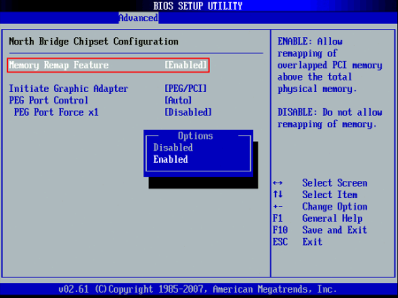
Why does this setting exist? The chipset is capable of remapping RAM that conflicts with PCI MMIO regions to addresses above 4GB; this feature is useful when the operating system supports accessing that RAM, such as a 64-bit operating system or a 32-bit operating system with PAE support. For more information, see here and here.
However, what is less comprehensible is why the default behavior is to unmap RAM between 3GB and 4GB entirely. While it is true that disabling physical addresses that conflict with PCI MMIO regions is more costly than necessary due to poor granularity of the disabled regions, it would seem that allowing the remaining memory to at least be counted and allocated to the extent possible would be a reasonable default behavior. Instead, the system pretends that RAM between 3GB and 4GB does not exist at all. Is there a reason for this? Inquiring minds want to know!
Edit: It appears that enabling this setting remaps the physical region from 2GB-4GB to be addressible starting at 4GB instead (only accessible by a 64-bit OS). With it disabled, the OS will be able to use up to 4GB of RAM that is not covered by PCI MMIO address space. In the case of this system, I had forgotten about the GPU RAM! So with Memory Remap turned off, more than 1GB of PCI address space was overlapping physical memory and rendering it unusable to the system. Mystery solved!
CPU upgrade note
The fastest CPUs available for the P5B-E are the Core 2 Extreme ‘Kentsfield XE’ series. These are quad-core processors with a 130W TDP. The QX6800 and QX6850 are very similar; the only difference is the FSB (1066MHz and 1333MHz respectively). However, the Intel P965 platform limits the FSB to 1066MHz, which makes the QX6800 the fastest available processor for the P5B-E. This processor can now be obtained on eBay for $50 or less.
Another reason the QX6800 is a good choice for the P5B-E is because the clock multiplier is unlocked. The reason this is a beneficial feature in a non-overclocking scenario is a bit obscure.
The Intel P965 chipset does not allow a downward memory multiplier. In effect, this means that the memory cannot run at a slower clock speed than the CPU FSB.
The fastest RAM the P5B-E supports is DDR2-800 (PC2-6400). To use DDR2-800 RAM at 400MHz, the CPU FSB must thus be set at 400MHz (1600MHz).
However, to run a multiplier-locked 1066MHz CPU at a 1600MHz FSB would become more difficult with higher multipliers due to the leveraging effect. If the QX6800 were multiplier-locked, its 11X multiplier would cause it to be clocked at 4.4GHz, which is at the very top end of what is possible on the Core 2 platform. (There are other considerations for scaling the FSB upwards such as the how the manufacturer implemented northbridge strapping: see here and here.)
Fortunately, since the QX6800 is multiplier-unlocked, it can be run at at a close-to-stock 7x or 8x multiplier to yield a 2.8Ghz or 3.2GHz clock speed. This will not require special cooling considerations for the CPU, but will allow DDR2-800 RAM to operate at its rated speed. This would otherwise be impossible with a high-end, multiplier-locked Core 2 CPU!
P5B-E board revision and CPU FSB
There are at least two revisions of the P5B-E mainboard. Rev. 1.02G adds the ability to adjust the northbridge, southbridge, and ICH voltages:

The northbridge voltage is the most important; it is difficult to attain a CPU FSB above 350MHz on the P5B-E without being able to increase the P965 NB Vcore from the default 1.25V, although the very similar P5B has possibly seen some better results. Therefore, if you have a Rev. 1.01G P5B-E, don’t bother trying to increase the CPU FSB beyond 350MHz or so.
At a 350MHz CPU FSB, you have two choices for the RAM speed: 700MHz and 875MHz. If DDR2-800 RAM is not stable at 875MHz, options are to loosen the timings or increase memory voltage. For example, if the memory is rated for 4-4-4-12, try 5-5-5-15 instead. Increasing the memory voltage may help stability, but the tradeoff is greater heat generation; RAM with small heat spreaders is often rated up to 2.1V, and RAM with large heat spreaders can likely tolerate more. If neither of these options result in a stable system, or the system will not boot at all at 875MHz regardless of timings, then the final option is to decrease the RAM clock to 700MHz.
At a 350MHz FSB, the closest CPU multiplier to stock will be 9x, to run the QX6800 at 3.15Ghz. Again, the unlocked multiplier helps here in keeping the CPU close to stock speed, and thereby reducing the number of experimental variables in customizing for maximum speed.
In my case, I was able to initially run the QX6800 (SLACP) at a 320MHz FSB and 10X multiplier (3.2GHz) with air cooling and BIOS automatically-determined voltages. The DDR2-800 RAM was then able to operate at its native speed (at a 4:5 FSB:RAM clock ratio) and 4-4-4-12 timings. Increasing the FSB even to 333MHz began necessitating tradeoffs: the RAM was then nonfunctional at CL4 and had to be bumped to 5-5-5-15 or reduced to a 1:1 FSB:RAM clock ratio to even successfully POST. As for the CPU, an 11X multiplier for the CPU (3.55GHz) proved unstable in memtest86+ under air cooling.
Unfortunately, the G.Skill F2-6400CL4S-1GBPK RAM that came with the system — despite being marked 4-4-4-12 — proved unstable at 4-4-4-12 during kernel compilation, but worked at the SPD default CL5. Increasing the DIMM voltage to 1.9V as indicated on the G.Skill website — but not the DIMM label itself — provided stability sufficient to complete a multicore Linux kernel build. (One point of interest revealed by using decode-dimms to dump the SPD EEPROM data is that the tRC and tRFC timings differ between DIMMs that, while being marked with identical G.Skill model numbers, are via visual differences obviously sourced from different manufacturing batches.) Also, a consistently bad address was found in repeated memtest86+ runs on one of the DIMMs; this was disappointing in terms of quality, but the GRUB_BADRAM configuration to exclude the small bad region saved the day at least.
The P5B-E has at least two minor annoyances in an overclocking configuration. The smaller of these is that depending on various settings, RAM speed is sometimes reported incorrectly by the BIOS: for example, RAM running at DDR2-800 speed will be incorrectly reported as PC2-5300. (Using memtest86+ or a DMI tool will report the correct configured speed.)
The larger annoyance is that to compensate for increasing the CPU FSB speed without running the CPU itself at an infeasibly high speed, it is only possible in the P5B-E BIOS (even the last version 1807) to set a lower fixed multiplier, rather than to set a maximum multiplier. But by setting a fixed multiplier, SpeedStep dynamic clocking is disabled entirely by the BIOS. Not being able to utilize dynamic clocking results in even hotter operation and more power consumption at idle for this already-hot 65nm process CPU. A better option would have been to allow the user to set a maximum multiplier and for the BIOS to regenerate appropriate ACPI _PSS tables.
Alternatively, if it were possible to boot Linux at the minimum CPU speed (perhaps by defaulting to the powersave cpufreq governor), then the maximum speed could be limited through tunables for the ondemand cpufreq governor after boot. Unfortunately, the default governor is a compile-time option and is chosen as performance, at least on Debian kernels, so pursuing this option would necessitate maintaining a locally customized kernel.
initrd hacking
A compromise is available that could allow increasing the FSB clock while leaving SpeedStep enabled, which would normally produce an infeasible top CPU speed. If your system is stable enough at the otherwise-infeasible top CPU speed to at least boot an initrd, the initrd script can immediately replace the cpufreq governor with the powersave governor, which will set the CPU to its minimum speed. After the system is booted, a local init script such as /etc/rc.local can set the maximum stable CPU speed, before once again enabling the ondemand governor as in normal operation.
I made the following modifications to my system to change the governor as early as possible (it does not seem to be possible to change it any earlier, such as in early-boot where CPU microcode is loaded from the initrd):
Create /etc/initramfs-tools/scripts/init-premount/overclock (chmod +x):
#!/bin/sh
# Force all cores to lowest speed as soon as possible during boot
PREREQ=""
prereqs()
{
        echo "$PREREQ"
}

case $1 in
prereqs)
        prereqs
        exit 0
        ;;
esac

. /scripts/functions
# Begin real processing below this line
for cpu_policy in /sys/devices/system/cpu/cpufreq/policy*; do echo 'powersave' > ${cpu_policy}/scaling_governor; done
In /etc/initramfs-tools/modules:
# List of modules that you want to include in your initramfs.
#
# Syntax:  module_name [args ...]
#
# You must run update-initramfs(8) to effect this change.
#
# Examples:
#
# raid1
# sd_mod
cpufreq_powersave
Create /etc/default/cpufrequtils:
GOVERNOR="powersave"In /etc/rc.local (add this later after successfully booting at least once):
for cpu_policy in /sys/devices/system/cpu/cpufreq/policy*; do echo 3000 > ${cpu_policy}/scaling_max_freq; echo 'ondemand' > ${cpu_policy}/scaling_governor; doneAnd then finally, update the initrd:
# update-initramfs -k all -uUnfortunately, the results were pathetic. Above 300MHz FSB, Linux would not even completely boot through the initrd, regardless of CPU or FSB voltage settings. Between 280MHz and 300MHz, the initrd would finish, effectively removing the CPU as an experimental variable. However, Linux would crash as the normal system init scripts were running, indicating a remaining problem with the FSB clock. Only once the FSB clock was lowered to 280MHz could I successfully compile a kernel. The QX6800 CPU itself had no problem operating at 3.2GHz there, but without the ability to increase the northbridge voltage, it was impossible to get system stability above 280MHz FSB. Unfortunately, lowering the FSB this low also meant the RAM clock would be lowered with it in a massive tradeoff, since the RAM could not operate at any higher FSB:RAM clock multiplier. The result was that a kernel compilation in the overclocked configuration was only 4% faster than that in the nominal configuration, making this all mostly a mental exercise.
Conclusion
In the end, I left the CPU at the default 266MHz FSB so that SpeedStep could be utilized; I used a 2:3 FSB:RAM clock ratio to run the RAM at DDR2-800 speed; and set the RAM timings to 4-4-4-12 and the DIMM voltage to 1.9V. Trying to squeeze any more performance from the CPU and increasing the FSB speed both involved unacceptable tradeoffs.